

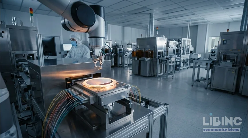
Indium Phosphide Photonics and the AI Data-Center Interconnect: A Quiet Bet in America's CHIPS Push
Table of Contents
In America's CHIPS push, the loudest headlines spotlight silicon logic and high-bandwidth memory. The Sherman project by Coherent shifts that focus. It is a $650 million expansion anchored by a government letter of intent that could channel up to $50 million in CHIPS funding to scale the world’s largest high-volume 150mm indium phosphide photonics facility. The aim is not to build more compute chips, but to harden the data highway that moves bits between GPUs, memory, and racks. AI workloads increasingly stall not on raw compute but on data movement and energy per bit. Indium phosphide photonics offers a path to move data with light, reducing latency and power at scale. This article unpacks why that matters and what it reveals about policy priorities and private investment signals.
Analytical view of indium phosphide photonics in AI data-center interconnects
The Sherman venture frames a long shot with outsized leverage. It targets the material platform that translates electrical signals into optical ones and then back again. Indium phosphide photonics, built on the 150mm wafer scale, enables lasers, modulators, and transceivers that form the data-movement backbone of AI systems. The project’s core is not the computation element but the interconnect fabric that binds compute, memory, and storage into coherent clusters. In economic terms, the bet rests on a bottleneck that shows up precisely as AI scales: the energy and latency costs of moving data across devices and racks. If the optical layer delivers, each GPU can operate closer to its peak without energy penalties that throttle throughput.
Why focus on interconnects now? Because the AI stack has evolved from a race to pack more transistors into a single die to a race to move more bits faster and cheaper. InP photonics promises lower latency paths and reduced power-per-bit than copper links over similar distances. This matters especially for next‑generation co-packaged optics and for the wider chassis where data must shuttle between accelerators and high-bandwidth memory. The analytical takeaway is simple: the interconnect is no longer a mere support system; it is a direct multiplier of compute efficiency. The term indium phosphide photonics recurs in every discussion of AI data-center efficiency because it marks a real shift in how data travels inside a cluster, not just how it is computed. InP devices are distinguished by their ability to function as integrated optical engines on a wafer, with potential gains in both performance and energy use.
- Capacity signal: Doubling the footprint and quadrupling wafer starts shifts supply dynamics for photonics hardware that has lagged behind silicon in scale.
- Technology signal: 150mm InP is not just a novelty; it is a pragmatic path to high-volume laser‑modulator‑transceiver integration on a mature wafer platform.
- Demand signal: Nvidia’s involvement links interconnect capability directly to co-packaged optics for data-center architectures, aligning private demand with public funding.
These signals converge on one central question: can a single line of Indium Phosphide photonics supply the interconnect discipline at the scale AI demands while keeping costs in check? The evidence so far suggests the potential is real, but the path is nontrivial. Ramp timelines, yield, and integration with existing silicon platforms will determine whether this becomes a durable capability or a bridging technology that slows down when the road gets hard. The data-movement angle remains the strongest argument for the investment; if optical interconnects deliver a meaningful reduction in energy per bit and latency, the entire AI stack benefits from a higher ceiling on cluster sizes and architectures.
The words of the industry are precise: indium phosphide photonics are essential for enabling high-speed data transmission within AI systems, telecommunications, and advanced networks. That assessment is not a marketing line; it reflects a fundamental architectural pivot—the belief that the bottleneck is not merely compute power but the speed and cost of moving data. The strategic implication is that the CHIPS program, by funding photonics alongside logic and memory, acknowledges the interconnect question in a way it historically has not. The Sherman project is a test of whether a government-led nudge can reorganize the private market’s attention toward a segment that has seen relatively modest capital compared with silicon-based compute.
Contrast with the logic-and-memory focus
The CHIPS program has poured the loudest capital into silicon logic and memory because those areas are the core levers of price-performance in modern computing. The Sherman expansion sits in a different quadrant: a small but strategic bet on the optical layer that binds a data center together. The funding structure clarifies the asymmetry. A federal allocation of up to $50 million sits atop roughly $20 million in state and local incentives and a much larger private investment from Nvidia that dwarfs the public sum. In summary, public capital here is catalytic: it signals and de-risks a private bet that private players had already identified as valuable.
From a technology perspective, the contrast is stark but informative. Silicon logic remains the primary engine of AI compute; Indium Phosphide photonics targets the communication fabric that enables those engines to scale. The private deal with Nvidia signals a concrete architectural direction: co-packaged optics that place the optical engine next to the switch or compute silicon. This is not just a packaging improvement; it is a rethinking of the interconnect topology. If the co-packaged approach holds up in scale, the data-center can push more GPUs into a network with lines that consume less energy per bit and operate with lower latency. The public policy takeaway is equally pointed: government funds will be most effective when they support the edges of the stack where private demand has already converged on a bottleneck. The optics bet, though smaller in dollar value, is where the AI data-path heat is hardest to dissipate and most worth de-risking.
- Scale contrast: Logic/memory fabs dwarf the photonics expansion in dollars, but the photonics component addresses a critical constraint that limits overall system throughput.
- Strategic pairing: Nvidia’s investment aligns the photonics supply with a major customer’s architecture roadmap, turning supplier capability into a strategic asset for data-center builders.
- Policy signaling: A small, targeted CHIPS investment in photonics signals a broader willingness to diversify the stack beyond compute power alone.
The practical implication is that the most transformative AI data-center improvements may come not from bigger chips but from smarter data highways. InP photonics, with its proven potential for high-bandwidth, low-latency photon-based interconnects, could be the enabler of more aggressive co-designs between GPUs, memory, and accelerators. The contrast underscores a broader assessment: policy is beginning to recognize interconnects as a critical performance lever rather than a background discipline.
Cause-and-effect relationships driving the bet
The Sherman investment ecosystem illustrates how cause and effect propagate through public policy, corporate strategy, and supplier capability. Nvidia’s $2 billion strategic investment and multiyear purchase commitments create a guaranteed demand window for Coherent’s photonics line, making the 150mm InP expansion economically sensible. This private demand acts as a high-confidence signal that the market is ready to absorb such capacity, which in turn justifies the public risk of a relatively modest grant. The CHIPS Program appears to recognize a bottleneck in data movement that typical chip-scale bets miss. By funding the optical layer, the program broadens the scope of resilience in the supply chain, reducing the risk that AI deployments stall for interconnect reasons even if compute keeps improving in silicon.
The optical backbone is not a peripheral add-on; it is a critical constraint on the AI data path. The cause-and-effect chain looks like this: private demand signals lead to a strategic alignment between supplier capabilities and customer roadmaps; public funding provides a catalytic nudge to scale and de-risk that alignment; and the resulting expansion in indium phosphide photonics capacity translates into a more robust data movement fabric. If the ramp succeeds, the data-motion wall becomes a less binding constraint, enabling larger, more energy-efficient AI clusters. If it stalls, the fragility of a single anchor supplier and a narrow high-value customer base becomes the central risk to the entire bet.
- Demand-to-capacity link: Nvidia’s commitment creates a near-term demand floor that justifies capital expenditure in a specialized fabrication line.
- Rationale for public funding: The federal grant acts as a signaling device to other potential customers and suppliers about the strategic value of photonics in the AI stack.
- Risk concentration: A single anchor supplier tied to a single anchor customer concentrates the program’s success on a narrow axis, raising systemic risk if the roadmap shifts.
The causal logic thus supports a nuanced reading: the investment is small in dollar terms but disproportionately leverages the interconnect layer, which has been underfunded relative to logic and memory. The result could be a quiet but meaningful improvement in data-center efficiency, provided ramp and integration challenges do not erode the economics. The risk-reward balance hinges on manufacturing performance, yield, and the ability to integrate InP devices with silicon-based systems at scale.
Expert reconstruction: implications for suppliers, policy, and engineers
From an expert’s vantage point, the Sherman project serves as a living stress test for how AI hardware supply chains adapt to bottlenecks beyond compute. If successful, it rewrites the prioritization map for capital expenditure within the CHIPS portfolio, elevating photonics from a niche supplier of optoelectronic components to a core enabler of AI data-center throughput. For suppliers, the message is clear: invest in scalable photonics platforms that can run on mature wafer lines and integrate with silicon ecosystems. For policymakers, the project demonstrates the value of targeted, capability-building grants that align with private demand signals, potentially guiding future program design toward more diverse choke-points in the stack. For engineers and system architects, the lesson is pragmatic: architecture must account for the optical interconnect path as part of the data-plane performance budget, not as a retrofit afterthought.
In practice, the differential between success and failure will hinge on four dimensions. First, ramp reliability: can a 150mm InP line sustain the quadrupled wafer starts without sacrificing yield? Second, integration discipline: how well do InP devices cohabit with CMOS logic and high-speed memory on the same platform? Third, supply-chain breadth: does the single-anchor model erode resilience if Nvidia’s roadmap shifts or if Coherent faces unforeseen production challenges? Fourth, economics: do energy-per-bit improvements translate into meaningful TCO reductions at data-center scale? Addressing these questions will determine whether this modest federal bet becomes a durable amplifier of AI throughput or a difficult-to-scale pilot with limited long-run impact.
In the end, indium phosphide photonics is not trying to replace silicon compute; it is trying to accelerate the data pipes that feed it. The Coherent-Sherman-Nvidia triangle embodies a deliberate shift in the AI hardware playbook: fund the optical backbone, and you unlock more ambitious compute architectures. If the optics bet proves robust, a future data center may look less like a sea of silicon and more like an integrated optical network where data moves through light as a routine design parameter, not an afterthought. That, more than any single wafer or grant figure, would mark a meaningful stride in the ongoing reconfiguration of the semiconductor ecosystem.
Key takeaway: the real leverage in the CHIPS program may lie in funding the optical layer that moves data, not just the chips that compute it. Indium phosphide photonics, though lower in headline value, sits at the critical juncture where AI performance actually scales, and where policy can nudge industry toward a more resilient, energy-efficient future.
Expanded View: From Demand Signals to Real-World Interconnects
Real-world ramping of 150mm InP photonics hinges on yield stability, seamless silicon integration, and a diversified customer ecosystem. Practical progress depends not only on a new fab but on reliable packaging, standardized interfaces, and multi-vendor resilience that reduce dependency on a single supplier or contract. These operational realities shape whether the optical interconnect becomes a durable component of AI data centers or a passing efficiency program.
| Technology | Latency | Power per bit | Maturity | Notes |
|---|---|---|---|---|
| Copper interconnects | Low to moderate | Higher energy per bit at scale | Mature | Widely deployed; robust short-reach links |
| Silicon photonics | Low | Lower energy per bit at high speed | Mature | CMOS-compatible; established supply chains |
| InP photonics | Very low | Lower energy per bit at scale | Growing | High integration potential for optical links |
| Co-packaged optics | Very low | Very low | Emerging | Key path for AI data paths; depends on supply chain |
The middle of the analysis emphasizes the practical obstacles: ramp reliability, device yield, and the need to harmonize InP devices with CMOS drivers and high-speed memory. Without repeatable yield and easy integration, even strong demand signals may not translate into durable capacity. This is where standard testbeds, cross-vendor packaging, and clear reliability targets become decisive enablers for long-run success.
Beyond energy, the architectural payoff comes from enabling tighter co-design between GPUs, memory, and accelerators. With reliable optical links near the compute fabric, designers can push higher bandwidth tiling, more aggressive memory hierarchies, and new data paths that keep latency low even as core counts rise. The practical implication is clear: the optical backbone becomes a central parameter in performance budgets, not a peripheral accessory.
| Aspect | Risk / Opportunity |
|---|---|
| Ramp reliability | Yield stability at scale is essential to lower cost per bit |
| Integration | Thermal and EMI management with CMOS interfaces |
| Supply chain | Diversified fabs reduce single-point failure |
| Economics | Capex amortization vs energy savings; long-run TCO |
In practice, the optics bet hinges on achieving consistent ramp plans, robust cross-compatibility, and a balanced ecosystem of suppliers and customers. When these conditions align, the optical layer becomes a durable multiplier for AI throughput, rather than a temporary efficiency push.
What is the role of InP photonics in AI data-center interconnects?
InP photonics enables high-bandwidth optical links that move data between GPUs, memory, and storage with lower energy per bit and reduced latency. In practical deployments, this translates to faster model updates, tighter integration of accelerators, and lower cooling loads in large-scale AI environments. For data-center ecosystems, success depends on reliable manufacturing, scalable packaging, and a diversified customer base that supports sustained demand.
Analytically, the optical interconnect layer acts as a lever to scale throughput while controlling energy costs, which is essential as model sizes and data movement requirements grow.
What are the primary cost and risk factors in scaling 150mm InP photonics?
The main costs include building and operating a 150mm InP fabrication line, managing device yield, and packaging for high-volume deployment. Risks involve a concentrated supplier base, integration challenges with silicon CMOS, and uncertain long‑term demand. A broader supplier ecosystem, clear roadmaps from major customers, and cross‑industry standards help align economics with risk management.
In depth, the financial payoff requires predictable yields and durable packaging interfaces, otherwise the capital expenditure may not translate into expected energy savings at scale.
How does co-packaged optics affect data-center energy efficiency?
Co-packaged optics can dramatically reduce energy per bit by shortening data paths and enabling higher switching densities. The direct effect is lower cooling and total cost of ownership for AI clusters. Real gains require reliable optical interfaces, robust thermal management, and consistent manufacturing yields across multiple supply chains.
The operational benefit compounds as clusters scale, making co-packaged optics a central element of energy-aware AI deployments.
What timelines are realistic for ramp and yield?
Realistic timelines balance fab ramp, yield improvement, and packaging maturation. Pilot lines may show early results within 1-2 years, with broader adoption over 3-5 years as processes mature and standardization advances. Milestones tied to specific performance metrics help guide expectations and investments.
This phased approach reflects the complexity of moving from pilot to mass production in a niche wafer technology.
How should suppliers and policymakers act to mitigate risks?
Suppliers should diversify fabrication assets, share repeatable yield data, and invest in packaging ecosystems. Policymakers can extend targeted grants to build scalable photonics platforms and push for standards that reduce integration risk across silicon and optics. The aim is to align incentives with measurable performance gains and supply resilience.
Strategic coordination, transparent data, and long‑cycle investment processes are essential to convert private demand signals into durable capability upgrades.
What metrics indicate successful implementation?
Successful implementation shows lower data-path energy per bit, reduced latency, and higher overall AI cluster throughput without compromising reliability. Additional indicators include ramp yield, time-to-scale, and TCO improvements per petaflop across representative workloads.
In practice, these metrics should be tracked across a diversity of AI workloads to verify consistency of gains and to inform ongoing optimization efforts.





Add a comment
To comment, you need to register and authorize
Comments
A deeper thread concerns the timing and sequencing of benefits. Interconnect improvements must be matched by software architectures, compiler strategies, and memory hierarchies that actually leverage lower latency and lower energy. If chip designers adopt tighter co-design with optical layers, the resulting system could reach peaks of efficiency that are simply not realizable with copper or with discrete optics. But the transition is nontrivial: packaging complexity, thermal coupling, wafer-to-wafer alignment, testing throughput, and yield management all become critical cost and reliability drivers. The discussion thus extends beyond physics into manufacturing strategy and policy calibration: should public funding emphasize not only the capability to produce larger fabs but also the ability to integrate new materials with established CMOS lines? And how should program targets be defined so that success translates into deployable improvements rather than a best‑in‑class pilot that never scales? These questions anchor a broader normative claim: if interconnects are the hidden rails of AI scale, then the governance of that rails deserves the same engineering discipline applied to the silicon cores. The comments here invite stakeholders to examine not just the potential winners, but the system dynamics that will determine whether a 150mm InP line becomes a durable enabler of globally distributed AI compute, or a valuable footnote in the history of semiconductors.