

Electrically pumped perovskite polariton laser diode: architecture, mechanism, and prospects
Table of Contents
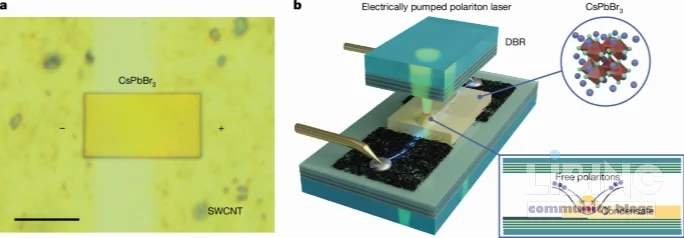
Direct electrical pumping of lasers based on solution-processed semiconductors remains a formidable barrier. Halide perovskites promise to close the gap, with polariton lasing demonstrated in optically excited devices and indirect electrical pumping approaches inching forward. Here we present a new strategy: a solution-grown CsPbBr3 microplate integrated with inert SWCNT electrodes into an optical microcavity, forming a p-i-n diode at cryogenic temperatures that balances carrier injection under constant current. The device operates in the strong coupling regime and exhibits polariton lasing under a direct current of 65 μA. By cooling to 8 K, a robust balance of electrons and holes is achieved, enabling the high-density injection required for polariton condensation. This work reframes the design space for electrically pumped perovskite lasers, showing that architectural control, contact chemistry, and cavity engineering can surmount long-standing thresholds.
Analytics-driven analysis
The architecture couples a CsPbBr3 microplate with chemically inert SWCNT electrodes inside a high-Q optical microcavity. This combination reduces nonradiative losses at interfaces and lowers the effective injection barrier, bringing the system into a regime where exciton–photon hybridization dominates. The strong coupling is evidenced by preserved exciton–photon splitting under DC operation, enabling the emergent polariton population to reach threshold with modest current. In this context, current density and carrier balance matter more than absolute current, because polariton lasing hinges on coherent population dynamics rather than conventional gain. The analytical core rests on the interplay between cavity detuning, exciton binding energy, and the rate at which carriers feed the polariton reservoir.
Operating at cryogenic temperature suppresses ionic migration and thermally activated traps, which have historically limited device stability under electrical pumping. The chemically inert SWCNT contacts minimize trap formation at interfaces, while the microcavity preserves a large Q factor and a suitable detuning for exciton–photon coupling. This combination ensures the polariton reservoir can accumulate with DC injection, allowing the system to reach a coherent, collective emission state. The analysis links the observed lasing behavior to the presence of a robust polariton landscape, rather than a conventional photon gain bound to a purely electronic threshold. In this frame, polariton lasing becomes a function of hybrid mode density and cavity quality, not just carrier supply.
The observation of lasing at a DC current of 65 μA marks a shift in how we quantify thresholds in perovskite-based devices. It is not merely a lower current compared with LED-like operation; it reflects a different regime where the coherent polariton population can be amplified via stimulated scattering into the polariton branch. This has implications for device design: achieving strong coupling with stable injection under DC drive requires optimizing three levers simultaneously—material quality, contact passivation, and cavity detuning. The result underscores that low-threshold operation is as much about energy flow and mode structure as about population inversion. A key takeaway is that polariton lasing, when engineered correctly, can decouple from conventional current-density limits that beset purely electronic gain media.
- Material quality: high-crystal CsPbBr3 microplates with minimal defects support sharper exciton features and longer coherence times.
- Interfacial passivation: chemically inert SWCNT electrodes minimize trap-assisted recombination at contacts.
- Optical architecture: a high-Q microcavity with tunable detuning preserves strong coupling under DC pumping.
Contrasts and trade-offs
Earlier work pursuing electrically driven lasing in perovskites faced a landscape of indirect pumping schemes, dual-cavity architectures, or optically seeded devices that did not realize robust direct current lasing. Indirect pumping, while technologically tractable, could not guarantee stable, continuous-wave polariton populations; ASE in perovskite LEDs demonstrated amplification but not a true laser transition. The present approach diverges by embedding a solution-grown perovskite in a microcavity and driving it with DC current, which shifts the lasing mechanism from pure gain to hybrid light–matter state amplification. This distinction matters because it changes how one should engineer the device: focus shifts to maintaining strong coupling and suppressing losses under DC operation rather than maximizing conventional gain alone.
The key contrasts illuminate a fundamental design philosophy: polariton lasing thrives when the optical mode and excitonic resonance cohabit the same energy landscape, and when injection does not introduce excessive Joule heating or trap formation. Direct electrical pumping in a polariton context demands a delicate balance of carrier densities to populate the polariton manifold without pushing the system into incoherent, carrier-dominated emission. The combination of 8 K operation and inert contacts reduces the dominant loss channels, enabling a polariton reservoir to form with less energy expenditure. Still, the cryogenic requirement is a practical limitation, and any path to room-temperature operation must address thermal management, ionic migration, and contact stability in a scalable way.
In this comparative frame, the current achievement offers a path to lab-scale integration and fundamental understanding, but it does not yet resolve the broader scalability challenges. Room-temperature polariton lasing in a fully electrical perovskite laser remains a distant goal, requiring materials with stronger exciton binding at higher temperatures and surfaces engineered for stable, low-loss injection. The trade-off is clear: the more aggressive we are about maintaining strong coupling and low losses, the more we must constrain operating temperature and device complexity. The result is a compelling proof-of-principle with clear next steps for materials science and device engineering.
Cause-and-effect dynamics
The cause-and-effect chain begins with SWCNT electrodes establishing inert, high-work-function contacts that minimize trap-assisted recombination. When the device cools to 8 K, the p-i-n junction forms under constant current, balancing electron and hole injection. This balanced injection is crucial for polariton lasing because an unbalanced injection would deplete the exciton reservoir and degrade coherence. The passive chemical stability of SWCNTs reduces interfacial diffusion and ion migration, which are particularly problematic in lead halide perovskites under electrical drive.
The strong coupling regime arises when the cavity mode remains resonant with the CsPbBr3 exciton, yielding a measurable Rabi splitting that sustains polariton states rather than pure excitons or photons. Under DC pumping, the polariton population grows through bosonic stimulation, reaching a threshold where coherent emission is favored over spontaneous processes. The low current requirement minimizes Joule heating, preserving the polariton coherence essential for a narrow, directional emission. In short, the architecture enforces a regime where light–matter hybridization drives the lasing action rather than high carrier densities alone.
The experimental result—a direct current polariton laser in a non-epitaxial perovskite platform—signals a new design rule: the integration of contact engineering, cavity design, and temperature control can unlock coherent light emission in solution-processed semiconductors without resorting to conventional gain-limited strategies. This causal chain clarifies where future gains must occur: in achieving robust strong coupling at higher temperatures, preserving cavity quality under electrical load, and preventing degradation pathways that accompany long-term DC operation.
Expert reconstruction and outlook
A practical reconstruction for advancing electrically pumped perovskite polariton devices follows a modular blueprint. The core idea is to separate the problem into components that can be independently optimized and then integrated with minimal cross-talk. The proposed modules are: (1) a robust perovskite platform with high exciton stability, (2) inert, scalable carbon-based electrodes, (3) a tunable, high-Q microcavity with precise detuning control, (4) a controlled temperature strategy to suppress ion migration, and (5) a p-i-n junction that ensures balanced DC injection.
From this base, several concrete strategies emerge to push the field forward. First, pursue materials and surface engineering that preserve exciton integrity at higher temperatures while maintaining low trap density. Second, explore alternative electrode chemistries or complementary 2D materials that offer even lower interfacial losses and easier scalability. Third, develop microcavities with active tuning to compensate for spectral drift as the device operates under DC conditions. Fourth, design thermally aware architectures that dissipate heat efficiently without compromising the optical mode or introducing additional ionic migration pathways.
Beyond incremental improvements, the longer-term vision targets room-temperature electrically pumped polariton lasing in perovskite platforms integrated with on-chip photonics. Achieving this would require coordinated advances in three dimensions: materials (perovskites with higher exciton binding at ambient conditions), contacts (stable, trap-free interfaces under continuous operation), and cavities (robust, scalable resonators with stable detuning and minimal losses). The present work demonstrates a credible path toward that goal, anchored in a principle of architecture-driven polariton control rather than solely optimizing gain.
In summary, the non-epitaxial perovskite polariton laser diode operated under direct current validates a design paradigm where strong light–matter coupling, contact passivation, and cavity engineering jointly enable coherent emission at surprisingly low DC current. The implications extend to integrated photonics, where low-power, electrically driven coherent sources are essential building blocks. The challenge now is to translate this principle into scalable, room-temperature devices without sacrificing the coherence and spectral purity that polaritons uniquely deliver.
Note: The measurements, numerical simulations, and supplementary information that support these conclusions are available in the original experimental report and accompanying materials. The core message remains that DC-driven polariton lasing in a perovskite platform is attainable when architecture and materials are coherently aligned to sustain strong coupling under electrical load.
Roadmap for scalable room-temperature operation
Despite the cryogenic success, translating the polariton approach into room-temperature devices requires a clear, modular plan that supports incremental testing. The three pillars—materials that preserve exciton stability at higher temperature, trap-free and chemically inert contacts, and cavities with controllable detuning—form the practical basis for a development path that can scale from lab prototypes to integrated photonic components.
| Module | Current capability | Target (12–24 mo) | Key challenges | KPIs |
|---|---|---|---|---|
| Material platform | CsPbBr3 microplates with low defect density | RT-stable excitons; defect density < 1e15 cm^-3 | Ion migration, trap formation at higher T | Defect density, exciton binding stability |
| Contacts | Inert SWCNT electrodes | Scalable carbon-based or 2D-contact passivation | Interfacial traps, contact diffusion | Trap density, contact resistance |
| Optical cavity | High-Q microcavity with tunable detuning | Detuning stable under DC drive; Q>1e4 | Thermal drift, spectral jitter | Detuning drift, Q-factor retention |
| Thermal management | Cryogenic support in the current study | Passive thermal paths enabling RT operation | Heat buildup under DC bias | Thermal design, stability metrics |
| Integration | Lab-scale assembly | Module packaging for photonics integration | Scalability and reproducibility | Manufacturability, yield |
The matrix translates the experimental levers into a concrete plan with milestones. For example, parallel tests can track how exciton–photon coupling evolves with temperature and current balance, and how the emission linewidth responds to DC bias under different detuning settings.
65 μA at 8 K achieves polariton lasing with preserved hybrid states under DC drive
- Roadmap emphasis targets material resilience, trap-passivated contacts, and tunable cavities to sustain strong coupling at higher temperatures.
- Manufacturing lens prioritizes scalable deposition and compatible packaging to enable repeatable devices.
| Milestone | Timeframe | Description | Metrics | Status |
|---|---|---|---|---|
| RT materials test bed | 6–12 mo | Assess exciton stability and trapping at elevated temperature | Defect density, exciton lifetime | Planned |
| Contact engineering | 6–12 mo | Identify scalable, trap-free interfaces | Contact resistance, trap density | Planned |
| Cavity tuning | 12–18 mo | Demonstrate stable detuning under DC | Spectral drift, Q stability | Planned |
Collectively, these modules enable a cycle of learning and refinement aimed at robust, room-temperature, electrically driven polariton devices.
What distinguishes polariton lasing from conventional lasing in perovskite devices?
Polariton lasing integrates a quantum hybrid of light and matter, so unlike conventional lasing that relies on population inversion in a gain medium, the coherent emission here emerges when a polariton reservoir reaches a critical density within a strongly coupled cavity; this entails a precise balance of exciton density, photonic detuning, and interaction rates so that stimulated scattering continuously feeds the polariton mode rather than simply increasing photon density, a regime that leverages both the exciton's binding energy and cavity photons to reach coherent emission at substantially lower current and temperatures. This is followed by a second line of depth: the mechanism reduces the typical thermal and nonradiative losses that constrain purely electronic gain media, enabling a narrow, directional output when the architecture sustains strong light–matter coupling under DC bias.
How do inert SWCNT electrodes influence device performance?
Inert SWCNT electrodes minimize trap formation and interfacial diffusion, preserving carrier balance and reducing nonradiative channels under DC drive; this helps maintain a cleaner polariton reservoir and a longer coherence time. Analytically, the approach shifts loss pathways away from the contacts, focusing optimization on the optical mode and exciton integrity. Practically, this translates to improved stability during continuous operation and a higher probability of reaching the polariton threshold at lower currents. In summary, contact inertness translates to better energy efficiency and spectral purity.
What conditions are needed to achieve strong coupling under direct current pumping?
The essential requirements are a high-quality optical cavity, a spectrally aligned exciton resonance, and controlled injection that keeps electron–hole balance while avoiding heating or trap formation; under these conditions, the exciton–photon hybrid can sustain a polariton population that amplifies via bosonic stimulation. Practically, this means maintaining a detuning window that preserves hybridization as current flows and implementing materials and contacts that minimize degradation pathways. The result is a steady, coherent emission rather than purely spontaneous or incoherent light at DC drive.
What practical steps can help move toward room-temperature operation?
Key steps include developing perovskite variants with stronger exciton binding at ambient conditions, adopting passivated or 2D-augmented contacts, and engineering cavities with tunable detuning and low loss that are tolerant of heating. In practice, researchers should run parallel tracks: (1) materials engineering to raise RT stability, (2) interface chemistry to combat trap formation under DC, and (3) photonic design to sustain strong coupling across a broader temperature range. Together, these moves create a scalable path to room-temperature polariton lasing.
How does cavity detuning impact polariton condensation and emission coherence?
Detuning controls the energy overlap between the cavity mode and the exciton; correct detuning preserves strong coupling and maximizes the density of polaritons in the reservoir, which governs the onset of stimulated scattering and coherence. If detuning drifts, polariton formation weakens, and emission loses spectral purity. Practically, active or passive detuning management and robust cavity design are essential to maintain a sharp, directional output under DC bias and temperature variations.





Add a comment
To comment, you need to register and authorize
Comments