

Table of Contents
- Lead
- Analytics on the semiconductor back end
- Contrast: Front-end growth vs back-end constraint
- Cause and effect: Packaging capacity and chip shipments
- Expert reconstruction: Rebuilding the domestic back end
- Conclusion
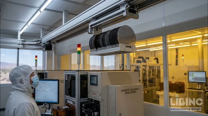
The semiconductor back end—the packaging, assembly, and test that turn a wafer into a finished device—has emerged as the choke point in today’s AI supply chains. Washington poured CHIPS-era capital into front-end lithography and wafer fabs, leaving the back end to the market. The result is a geography mismatch: domestic wafers, offshore finishing, and an air-freight loop that turns a near-complete product into a trans-Pacific shipment. This is not a minor inefficiency; it is a structural constraint that determines whether the most valuable chips actually ship.
Understanding the back end as the binding constraint reframes policy debates and corporate bets. The most valuable AI accelerators rely on advanced packaging—CoWoS-based interconnects that merge logic with high-bandwidth memory. Asia dominates OSAT capacity, and even ambitious U.S. projects must contend with substrate lead times, interposer supply, and a workforce trained for a highly specialized craft. The analysis that follows quantifies the bottleneck and sketches what it will take to rewrite the flow from wafer fabrication to shipped chip, without pretending that new fab footprints alone suffice.
Analytics on the semiconductor back end
The global back end, formally outsourced semiconductor assembly and test (OSAT), sits at the intersection of capability and logistics. Market-research estimates for 2025 place Asia-Pacific at roughly 74% of OSAT capacity, with North America about 15%, Europe near 8%, and the Middle East and Africa around 3%. Those proportions are not a coincidence; they reflect decades of capex allocation, supplier ecosystems, and workforce specialization. In other words, even after reshoring rhetoric and CHIPS Act incentives, three-quarters of the world’s chip assembly and test sits in Asia. The geography is not accidental; it is the outcome of policy choices and market incentives that favored front-end capital over the back end.
The bottleneck has shifted from lithography to packaging. CoWoS—Chip-on-Wafer-on-Substrate—interposers have become the critical enabler for AI accelerators by stacking memory, logic, and high-speed interconnects in a single package. The issue is not merely throughput, but the availability of substrates, interposers, materials, and the skilled technicians who actually run the line. Where a fab can produce logic wafers, a functioning CoWoS line is what turns those wafers into ships. When TSMC’s Taiwan packaging capacity runs near full through 2025, the limiting step moves from writing masks to delivering a finished device that can be soldered onto a board.
Amkor’s Peoria campus is the domestic answer to this bottleneck. The project expanded to $7 billion across two phases, anchored by Apple and Nvidia as first- and second-tier customers. The plan envisions more than 750,000 square feet of cleanroom space and as many as 3,000 jobs. The first manufacturing facility is scheduled to complete in mid-2027, with production beginning in early 2028. The numbers matter less than the implication: even a large domestic back end is a two-year lead-time project, and it does not immediately erase dependence on trans-Pacific packaging lines.
Contrast: Front-end growth vs back-end constraint
The CHIPS Act famously favored the capital-intensive, marquee end of the business—fabrication and lithography—over the back end where the value actually becomes a usable product. The logic was clear: build world-class wafer fabs to reduce dependency on foreign suppliers for the most visible, high-margin step. But the economic and technical bottleneck has moved to packaging and test. The same policy that funded front-end fabs created a misalignment with the real market constraint for AI accelerators: the ability to finish and ship the chips. Packaging is not an afterthought; it is the last mile, and its constraints determine whether a fab’s output ever reaches a customer’s board.
Asia’s dominance in OSAT confirms the risk. The Osat ecosystem includes substrate and interposer suppliers, specialized materials, and a trained workforce that treats packaging as a distinct industrial discipline from wafer fabrication. The result is a supply chain with long lead times and intricate dependencies. The 2025 market fragmentation underscores this: even with U.S. wafer production, the finish remains abroad unless domestic packaging scales with equal velocity. A package must be designed and manufactured in the same ballpark as the die it carries; otherwise, the assembly line is a bottleneck rather than a bridge to production.
- Policy alignment with back-end needs to be explicit, not incidental.
- Supply-chain resilience requires substrates, interposers, and packaging equipment made or sourced domestically.
- Workforce development must be parallel to capex, not after the fact.
Cause and effect: Packaging capacity and chip shipments
The practical consequence of the back-end bottleneck is an air-freight loop. Wafers move from U.S. fabs to Taiwan for dicing, test, and packaging, then return as finished chips that must be soldered onto boards worldwide. This is not a mere inefficiency; it is a systemic constraint that shapes the AI supply chain’s speed, cost, and reliability. The CoWoS bottleneck in particular pins chip output to the availability of advanced packaging lines. If you cannot place a CoWoS line in the same region as the die, shipments stall even when fabs are running at or near capacity.
The internal logic is straightforward: packaging lead times and interposer availability translate directly into on-time delivery risk for AI accelerators. Substrates and materials complicate the window further. If substrate supply tightens, or if skilled packaging technicians cannot be trained fast enough, even a fully modern wafer fab cannot convert capacity into actual shipments. The result is a dependency loop that the U.S. is only beginning to address with Amkor’s Arizona campus and TSMC’s in-state packaging ambition.
Looking ahead to late 2027 and 2028, the timing will be decisive. If Amkor’s mid-2027 construction completes and early-2028 production starts, and if TSMC's in-state packaging target also meets its milestones, Arizona could host a genuinely all-American end-to-end flow for certain high-value chips. But this outcome is not guaranteed. Lead times, supplier capacity, and a trained workforce remain structural constraints, not one-off hurdles. The bottleneck is not the lithography press—it's the packaging line that slips or accelerates independently of photomask sales.
Expert reconstruction: Rebuilding the domestic back end
The path to a self-contained domestic back end is not a single investment; it is a re-engineering of a whole ecosystem. In practical terms, the U.S. would need parallel advances in three domains: packaging facilities, substrate and interposer supply, and the workforce that runs the lines. The steps are interdependent and time-sensitive:
- Stand-up of multiple packaging facilities with scalable cleanrooms and flexible lines that can handle high-bandwidth interconnects.
- Resilient substrate and interposer supply through domestic or nearshore sources to reduce lead times and currency risks.
- Workforce development programs that quickly train technicians, engineers, and process specialists for advanced packaging disciplines.
TSMC’s parallel move toward in-state packaging signals a broader shift: advanced packaging is now a strategic capability, not a geographic afterthought. Amkor’s Peoria campus shows what a scaled, domestically anchored OSAT operation looks like on paper, but the operational ramp—how to recruit and retain a skilled workforce, how to source substrate and materials at scale, how to sequence equipment upgrades to avoid downtime—will determine whether the U.S. can sustain a 7+-billion-dollar investment without external bottlenecks.
For policy and industry to accelerate, the following levers are essential:
- Targeted funding for back-end ecosystems that align with wafer fab investments.
- Strategic supplier development for substrates, interposers, and packaging equipment to reduce dependency on foreign markets.
- Talent pipelines built around packaging science, materials, and process engineering, with clear pathways from apprenticeship to leadership roles.
In the end, the shift from a geography-dominated OSAT to a domestically integrated back end hinges on the ability to knit together supply, capital, and people into a reliable, repeatable manufacturing system. A single grand project cannot deliver this; a portfolio of actions that reinforces the entire chain is what will finally move the needle on all-American chips.
Conclusion
The fabs were the easy part. The back end is the test. Semiconductor back end capability—packaging, assembly, and test—has become the decisive factor that determines whether the United States can translate wafer fabrication strength into finished chips that actually ship. Without scaling domestic packaging and related supply chains, even the most advanced front-end fabs will fail to close the loop. The coming years will reveal whether Amkor’s Arizona campus, TSMC’s in-state packaging, and a broadened domestic ecosystem can finally reconcile the gap between wafer production and chip delivery. Until then, the AI supply chain will remain tethered to the trans-Pacific finishing lines that underwrite today’s global chip market.
Closing the domestic back end with a practical rollout plan
The most actionable improvement is a concrete, phased program that links wafer fabrication to ready-to-ship devices within the United States. Without this alignment, capacity gains in front-end do not translate into faster AI product cycles. A balanced plan must coordinate packaging, substrates, and workforce with capital, and include milestones and risk mitigations.
| Phase | Timeframe | Key Capex | Expected Outcome | Risks |
|---|---|---|---|---|
| Near-term readiness | 0–18 months | $2B | 1–2 pilot lines in domestically located packaging | Supply constraints |
| Mid-term scale | 18–36 months | $5B | 2–3 fully operational lines, established substrate pilots | Labor shortages |
| Long-term expansion | 36–60 months | $8B | Multi-site OSAT capability for select accelerators | Policy and currency risks |
| End-to-end domestic | 60+ months | $12B | Significant share of domestic shipments | Cost inflation |
Phase-driven actions provide a clear budget, timeline, and accountability framework. In practice, this means coordinating with substrate suppliers, training programs, and equipment suppliers to avoid downtime and minimize transfer costs between regions.
What is the semiconductor back end and why does it matter for AI chips?
In this context the back end includes packaging, assembly and test that turn wafers into finished devices. It matters because AI accelerators rely on tightly integrated die, memory, and high‑speed interconnects within a single package; without robust packaging capacity, even advanced wafers cannot ship in volume. This last mile governs delivery speed, cost, and reliability.
How does packaging capacity influence chip shipments and delivery timelines?
Packaging capacity sets the pace at which fab output becomes usable product. When lines are constrained, shipments slip and inventories swell. Practically, lead times from substrate to finished device can extend by weeks; nearshoring and domestic packaging reduce exposure to trans-Pacific bottlenecks and improve predictability.
What is CoWoS and why is it important for AI accelerators?
CoWoS stands for Chip-on-Wafer-on-Substrate. It stacks memory and logic in a single package to deliver enormous bandwidth in a compact form, which is essential for large AI models that need rapid memory access and energy efficiency in every chip.
What would a phased plan for domestic packaging look like?
Phase 1 focuses on near-term readiness: stand up a couple of lines, secure substrate pilots, and train technicians. Phase 2 scales multi-site packaging and solidifies suppliers. Phase 3 targets end-to-end domestic capability for select accelerators, guided by real-time data dashboards and risk management.
Which policy measures could accelerate domestic packaging capacity?
Targeted funding for OSAT ecosystems, streamlined permitting for packaging facilities, incentives for domestic substrate and interposer suppliers, and strong workforce programs accelerate capital deployment and reduce risk.
What are the main risks to building a domestic OSAT ecosystem, and how can they be mitigated?
Key risks include cost escalation, supply volatility, and skilled-labor shortages. Mitigations involve multi-site diversification, long-term supplier contracts, and public-private partnerships with clear milestones and accountability.





Add a comment
To comment, you need to register and authorize
Comments