

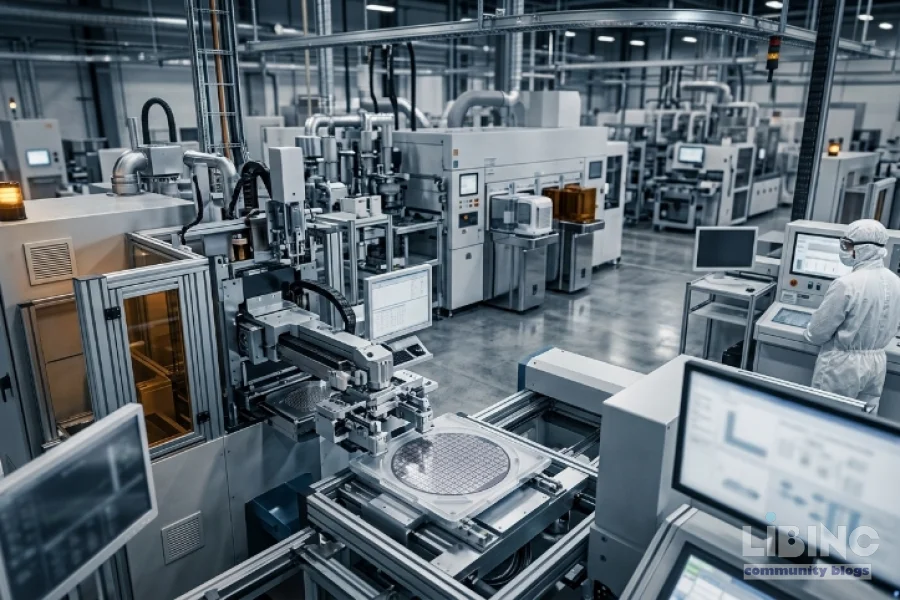
TSMC capex and packaging bottleneck: decoding May 12, 2026 approvals, Arizona funding, and the decoupling ceiling
TSMC's May 12, 2026 board meeting yielded US$31.28 billion in capital appropriations, plus an authorization of up to US$20 billion to capitalize TSMC Arizona. On the surface, the numbers read as a dramatic pivot: a large U.S. wafer-capacity injection and a clear signal that Washington is finally pulling meaningful share of leading-edge spending. In practice, the arithmetic hides a staged program. Appropriations are permissions, not cash outlays, and they stack on prior tranches rather than replacing them. The deeper constraint isn't the pace of new wafer fabs but the packaging loop that stitches silicon to systems—CoWoS, panel-level packaging, and memory interconnects—that to date remains anchored in Taiwan. This analysis reconstructs the story from headline totals to the physics of deployment, and asks what signals truly forecast 2026-2028 outcomes for supply-chain resilience.
Analytics: decoding the TSMC capex and packaging bottleneck in the May 12 numbers
Two large capex tranches arrived within three months, and both sit inside a broader capex envelope that exceeds the company’s own 2026 guidance. The February tranche, roughly US$44.96 billion, set a high watermark that the May US$31.28 billion addition reinforces rather than overturns. The effect is not a cash reallocation but a staged permission structure that expands the total pool available to fund front-end fabs, back-end packaging, and related tooling. The packaging loop remains the choke point because it governs how quickly wafer outputs translate into finished AI accelerators and systems. This is where capacity must align with demand, and where policy and geography interact with physics to constrain acceleration.
- Capex composition: TSMC has framed 2026 capex as roughly 70–80% for advanced logic nodes (N3, N2, A16), 10–20% for advanced packaging and mask making, and about 10% for specialty nodes. Arizona sits as a line item within that distribution, not a rival to it. This matters because advancing packaging capacity in the U.S. does not instantly translate into AI accelerator-ready products if the front-end cadence remains Taiwan-centric.
- Appropriations versus cash: Appropriations unlock future cash-outlays but do not deliver cash today. The real question is the timing and cadence of tool-ins, construction, and commissioning across multiple sites. In 2026, the pace of approvals outstrips immediate execution risk only if execution keeps pace with the schedule implied by these permissions.
- Mix implications: The 2026 mix—heavy on advanced process with a sizable, but smaller, advanced packaging allocation—means the bulk of incremental capacity still rides on Taiwan-based packages. Arizona accelerates wafer output for selected nodes but does not, by itself, sever the packaging’s dependence on Zhunan, Chiayi, and Tainan for CoWoS interconnects.
The push to N2 volume production in 2024–2025 and the 2026 rate hints that the next wave of tools and line-ups is already pre-committed. The February tranche was interpreted by many as a front-runner for 2nm tool-in; the May tranche extends that posture rather than reversing it. In other words, the cadence is accelerating the phosphorus of node transitions while preserving a fixed backbone of packaging throughput that remains Taiwan-bound in the near term.
Two additional data points matter for the analytics lens. First, the 2026 capex band guidance of US$52–56 billion already assumes a high, but not unlimited, level of front-end expansion. Second, the allocation inside that band shows a deliberate tilt toward 2nm ramping (with five fabs planned across Hsinchu and Kaohsiung) and a sustained push on advanced packaging (AP6–AP8) and CoWoS capacity growth toward roughly 130,000 wafers per month by late 2026. The math is simple: Arizona strengthens wafer supply, but the binding constraint remains the packaging chain that stitches devices to memory and interconnects. Without a parallel uplift in domestic packaging capacity, decoupling remains partial at best.
Contrast: Arizona injection vs Taiwan spend, the real allocation inside the capex pool
What happens when we separate the headline from the real allocation? The Arizona capital injection enters as a parent-to-subsidiary transfer into Fab 21’s operating entity. Trade press ties the money to Phase 2 acceleration, N3 tooling, and Phase 3 site work, all part of a sprawling Arizona roadmap. Yet the broader picture shows that the allocation within 2026 remains heavily weighted toward two activities: ramping 2nm nodes in Taiwan and expanding advanced packaging in Taiwan. The U.S. injection is a meaningful addition to wafer capacity, but it does not hollow out the Taiwan loop that feeds the packaging and interconnects necessary for AI accelerators.
- : The Phase 2 tool-in for N3 in Arizona targets 2027–2028, with 2H 2027 often cited as the milestone. That cadence aligns with 2nm ramp plans in Taiwan and does not alone unlock the CoWoS-based packaging critical path.
- : AP6 in Zhunan, AP7 in Chiayi, and AP8 in Tainan comprise the core advanced packaging push. CoWoS capacity growth toward 130,000 wafers per month implies that most AI accelerator packaging remains physically anchored in the Taiwan ecosystem, even as Arizona adds wafer capacity.
- : The CoWoS line is the gating resource for leading-edge AI accelerators. The CoPoS path, anchored in Taiwan and moving slowly toward scaling in 2028, confirms that the package is the real ceiling—policies and geography aside.
Japan’s role provides a counterpoint. Kumamoto’s JASM Phase 2 has slowed, with site tools pulled back and a potential 4nm consideration for trailing-edge nodes. The net effect is a diversification narrative that falters at the same choke point: packaging and assembly are not as readily redirected to the U.S. as wafer fabrication. In short, Phoenix accelerates wafer output; the Taiwan loop still controls the speed-to-market of actual AI accelerators.
Cause and effect: why packaging is the ceiling
The structural reason packaging caps the decoupling story is policy alignment, not physics alone. CHIPS Act subsidies sized the front end—the wafer fabs and the capital-heavy substrate that creates the die. Outsourced semiconductor assembly and test, and the advanced packaging adjacent to it, were never the focus of the subsidy architecture. That creates a practical ceiling on what a US$20 billion Arizona injection can buy in terms of supply-chain resilience: it accelerates wafer output but does not bring forward the date at which an AI accelerator can be fabricated, packaged, and tested without ever touching Taiwan.
Physically, the loop remains Taiwan-led. Even when a wafer is fabricated in Phoenix, it still returns to Zhunan, Chiayi, and Tainan for CoWoS interconnects. The next-gen panel packaging variant, CoPoS, looks to June 2026 for pilot completion, with volume ramp not expected until 2028. The result is a decoupling story that looks large in the headlines but is bounded in practice by the packaging buildings outside Chiayi and the memory interconnect ecosystem that binds the system to the silicon. The diversification narrative survives only because Phoenix is doing the heavy lifting on wafers, not on packaging.
- : Subsidies tilted toward front-end fabrication leave back-end assembly and packaging under-capitalized in policy terms, constraining U.S. leverage over the full AI stack.
- : Packaging lines cannot simply relocate; they require mature supplier ecosystems, skilled labor pools, and long-term supplier networks that Taiwan has refined over decades.
- : CoWoS remains the ultimate bottleneck, meaning many accelerators cannot exit the manufacturing cycle until packaging capacity expands in tandem with wafer production.
The upshot is stark: the CHIPS Act-sized the wrong layer goes beyond policy, anchoring the structural limit of what Arizona alone can deliver. The packaging ceiling, not the front end, governs the speed at which a truly resilient, US-anchored supply chain for AI accelerators can emerge. The decoupling of silicon from systems therefore remains partial, with the real leverage sitting in the packaging and assembly segments that are still Taiwan-centered in 2026.
Expert reconstruction: signals to watch and near-term policy levers
Four near-term signals will matter more than the next round of headline appropriations. They will reveal whether the chinks in the decoupling narrative are widening or narrowing as 2026 unfolds.
- : Earnings call commentary or vendor briefings that tilt the packaging allocation higher than the current 10–20% band imply the CoWoS ceiling is binding more tightly than disclosed and that Taiwan's packaging ramp could constrain H2 2026 outputs.
- : The H2 2027 target for N3 volume production in Arizona remains the key metric, not the size of the appropriation. Any delay or acceleration here will reframe the pace of overall decoupling.
- : A pivot to 4nm would reshape the trailing-edge map, potentially reducing the burden on Taiwan for certain maturities and altering the regional dependency matrix.
- : Whether TSMC revises the 2026 capex band upward beyond US$52–56 billion will signal confidence in Taiwan's packaging expansion and in the ability to reallocate investment between front-end and back-end capabilities under real-world constraints.
The cleaner read on May 12 is that TSMC is spending aggressively on both sides of the Pacific. The Arizona injection is real and meaningful for U.S. wafer capacity, but the decoupling story still has a hard ceiling—set not in Phoenix or Hsinchu, but in the packaging buildings outside Chiayi. If the near-term signals tilt toward greater packaging share and faster tool-in at Arizona, we may see the ceiling soften. If not, the structural limits will persist, and the narrative of partial decoupling will remain the operative frame for policymakers and investors alike.
In the end, the May 12 action represents a push on two fronts—accelerating wafer output in the U.S. and expanding the Taiwan packaging backbone. The first moves the world closer to a more resilient supply chain, the second preserves the dependency that determines how quickly AI silicon can be delivered to customers. The 2026 arc will hinge on how quickly the packaging loop can adapt, not merely how much capital the U.S. can conjure for Arizona.
What operators and investors should watch is not the next tranche of headline spend but the four signals above. The outcome will determine how much of the decoupling narrative becomes a durable structural shift versus a strategic reassessment of the current supply chain architecture.
Bottom line: TSMC’s 2026 capex push is multi-faceted and heavily staged. Arizona accelerates wafer output, but the packaging ceiling anchored in Taiwan remains the true determinant of any real pivot toward a US-centric AI silicon ecosystem.
Expanded analysis: practical implications for packaging resilience
While headline capex signals ambition, the binding constraint remains the packaging and interconnects that stitch wafers into AI-ready modules. To translate the main findings into actionable insight, consider three scenarios that illustrate timing and risk for delivery timelines in 2026–2028.
| Capability | 2026 Share | Major Focus Locations | Key Constraint |
|---|---|---|---|
| Front-end Fabs (N3/N2) | 70–80% | Taiwan; Arizona (Phase 2) | Yields, tool-in cadence |
| Advanced Packaging (CoWoS/AP6-AP8) | 10–20% | Zhunan, Chiayi, Tainan | CoWoS capacity ceiling |
| Specialty Nodes | 10% | Taiwan; Japan | R&D cycles |
| Arizona Wafer Capacity Injection | Included in front-end | Phoenix; Gigafab | Partial decoupling, not packaging |
- Capex 2026 band: US$52–56 billion
- Arizona injection: up to US$20 billion
- Packaging growth: CoWoS to ~130,000 wafers/month by late 2026
Interpretation: even with Arizona adding wafer headroom, the time-to-market for AI accelerators is still gated by back-end packaging and interconnects. A faster cadence in packaging would be a stronger signal of real decoupling. Investors should monitor near-term signals in the next reports for evidence of faster tool-in and higher packaging allocation beyond the current bands.
| Milestone | Target Window | Impact | Risks |
|---|---|---|---|
| Arizona Phase 2 N3 tool-in | H2 2027–2028 | Increases wafer supply | Delays in tooling or site readiness |
| CoWoS capacity ramp | 2026–2027 | Packaging throughput | Facility bottlenecks; supply chain variations |
| AP6-AP8 packaging expansion | 2026–2028 | Tier 1 AI accelerators | Labor and process maturity |
| CoPoS pilot completion | June 2026 pilot; 2028 full ramp | New interconnects | Technical risk; supplier readiness |
Bottom line: the practical path to resilience combines wafer expansion in the U.S. with a parallel, staged uplift in Taiwan's packaging engine. The four signals to watch—packaging mix commentary, Arizona tool-in timing, JASM Kumamoto updates, and capex guidance—will determine whether the decoupling narrative gains credibility in 2026–28.
What do the May 12 capex numbers imply for US supply chain resilience?
The May 12 numbers indicate a staged, multi-year push that adds wafer capacity in the United States while keeping most packaging activity anchored in Taiwan. This separation improves resilience only if the packaging lines in Taiwan can ramp in parallel or if the U.S. can accelerate domestic packaging capacity; otherwise, the real time-to-market for advanced AI silicon remains limited by CoWoS and related interconnects. In practice, investors should watch for packaging allocation trends andArizona tool-in progress as leading indicators of true decoupling progress.
Analytically, the capex mix suggests a dual-track strategy: stronger wafer supply in the U.S. paired with a steady Taiwan-based packaging backbone. This combination reduces geopolitical risk but preserves the current production cadence, making resilience contingent on back-end expansion as well as front-end growth.
Why is packaging considered the bottleneck, even with Arizona expansion?
Packaging bottlenecks arise because CoWoS and related interconnects are specialized, high-capacity processes that require mature ecosystems. Even if Arizona adds wafer capacity, the final AI accelerator must still be packaged and tested in facilities that rely on Taiwan’s established packaging supply chain. This means the time-to-market for new AI silicon depends as much on CoWoS capacity and memory interconnects as on wafer fabrication. Practically, reducing this bottleneck needs coordinated investments in Taiwan’s packaging lines and a faster tool-in cadence across the full supply chain.
From an investment perspective, a bottleneck at packaging translates to delayed revenue recognition for AI accelerators, even when wafers are plentiful. Monitoring CoWoS output and AP6–AP8 expansion progress provides a clearer read on potential delivery schedules.
How does the Arizona injection interact with Taiwan’s packaging backbone?
The Arizona injection raises wafer output in the U.S. but does not automatically accelerate packaging in the United States. The two efforts are complementary: more wafers can be turned into finished devices only if packaging capacity and interconnects are available at scale. In practice, Arizona’s Phase 2 tool-in in 2027–2028 aligns with ongoing Taiwanese upgrades; successful decoupling requires both tracks to advance in tandem. For stakeholders, the key is to verify milestones in tool-in, packaging ramp, and CoWoS throughput in near-term earnings or briefing calls.
What do AP6-AP8 and CoWoS mean for AI accelerator timelines?
AP6-AP8 represent a dedicated push to increase advanced packaging capacity, while CoWoS is the principal interconnect technology for high-end accelerators. Their combined ramp determines when AI chips can be packaged, tested, and shipped. If these lines accelerate in 2026–2027, the time-to-market could improve meaningfully; if not, the allure of U.S.-based wafer supply remains tempered by Taiwan’s packaging constraints. Investors should compare announced capacity targets with actual ramp rates in quarterly updates to gauge progress.
What are the near-term signals that the decoupling narrative is gaining credibility?
Key signals include an uptick in the packaging mix beyond the 10–20% band, earlier than planned Arizona N3 tool-in, faster Kumamoto Phase 2 updates toward 4nm mappings, and a capex trajectory that supports stronger back-end expansion. A visible shift in any of these areas would suggest a higher likelihood of reduced dependence on Taiwan’s packaging loop, strengthening the case for deeper resilience in the AI silicon supply chain.
What policy levers could accelerate domestic packaging and decoupling?
Policy levers include expanding subsidies or incentives specifically for back-end packaging facilities, streamlining permitting for new packaging plants, and fostering regional supplier ecosystems to shorten lead times for memory interconnects. Aligning CHIPS Act subsidies with packaging and assembly expansion would directly address the current misalignment between front-end funding and back-end needs. For stakeholders, policy alignment is a practical lever to shorten the path from wafer production to delivered AI accelerators.





Add a comment
To comment, you need to register and authorize
Comments